
Introduction
Electronic circuits form the backbone of modern electronic devices, from everyday gadgets like smartphones to advanced systems used in aerospace and medical applications. Given their critical role, it’s essential to evaluate their performance under various electrical and thermal conditions to ensure reliability and longevity.
Electrical stress analysis is a vital part of board design, aimed at preventing potential failures and enhancing overall performance. This guide offers an exploration of electrical stress analysis principles, methodologies, and tools, and discusses how integrating this analysis into your design process can significantly improve product reliability and robustness.
What is Electrical Stress Analysis in Board Design?
Electrical stress analysis involves evaluating the impact of electrical currents, power, voltages, and thermal conditions on components to ensure they operate within their safe limits. This analysis is essential for identifying potential failure points, optimizing component selection, and refining PCB layouts to prevent overstress and overheating.
By conducting thorough electrical stress analysis with specialized tools like BQR, engineers can anticipate and mitigate issues that might arise during the operational life of the board, leading to more reliable and durable electronic products.
Key Components of Electrical Stress Analysis
Component Selection
Selecting components with the appropriate electrical and thermal ratings is fundamental to ensuring board reliability. Datasheets provide crucial information about a component’s maximum power, voltage, current, and temperature limits. Engineers must carefully review these specifications to choose components that can withstand the expected operational conditions and avoid premature failure.

the derating guideline curve. Green region = operational stress is below the derating guideline curve.
Derating Calculations
Derating is the practice of operating components below their maximum rated limits to improve reliability and longevity. Electrical derating considers factors such as ambient temperature, voltage variations, and load conditions. By applying derating calculations, engineers can extend component lifespan and reduce the risk of failure due to overstress.
Power Integrity Analysis
Power integrity analysis ensures stable voltage levels and minimizes fluctuations that can stress components. It involves evaluating the board power distribution networks to identify potential issues such as voltage drops or noise that could affect performance. Maintaining power integrity is essential for reliable operation and overall system stability.
Thermal Simulation
Thermal management is critical for maintaining circuit performance and preventing overheating. Thermal simulation tools predict heat distribution across the PCB, identifying potential hotspots and areas where heat dissipation might be inadequate. Effective thermal management strategies, such as using heat sinks or improving airflow, can prevent component damage and ensure consistent performance.
Electrostatic Discharge (ESD) Protection
ESD protection is vital for safeguarding sensitive components from voltage spikes caused by electrostatic discharge. Implementing appropriate ESD protection measures, such as using TVS diodes or designing robust PCB layouts, can prevent damage and enhance the long-term reliability of the device.
Benefits of Electrical Stress Analysis
Investing in comprehensive electrical stress analysis offers numerous advantages.
Enhanced Product Reliability
Proactively identifying and addressing potential failure points results in more reliable and robust products. Electrical stress analysis helps engineers anticipate issues before they manifest, leading to fewer field failures and greater customer satisfaction.
Reduced Development Costs
By addressing potential issues early in the design phase, engineers can minimize costly rework and redesign cycles. Effective electrical stress analysis helps avoid unexpected problems that could lead to expensive delays and additional development costs.
Improved Product Safety
Mitigating risks associated with component overheating or electrical overstress enhances the safety of electronic devices. Thorough analysis ensures that products operate within safe limits, reducing the likelihood of safety hazards or malfunctioning.
Streamlined Regulatory Compliance
Designers of critical electronics are often required to comply with standards such as:
- European Space Agency (ESA): ECSS-Q-ST-30-11C
- NASA: EEE-INST-002
- NAVSEA: SD-18
These standards provide critical benchmarks for evaluating electrical stress, helping engineers design robust and reliable systems.
Electrical Stress Analysis Ensures Compliance with Industry Standards
By performing electrical stress analysis, engineers can verify that their designs adhere to industry standards and regulations, ensuring safety and optimal performance. This process facilitates smoother certification and approval.
Techniques and Tools for Electrical Stress Analysis
Manual Calculations
Manual calculations provide a fundamental understanding of electrical stresses. Engineers can use these methods to perform basic derating and thermal evaluations. However, for complex designs, manual calculations can be time-consuming and prone to errors.
Simulation Software
Advanced simulation software tools offer a more efficient approach to electrical stress analysis. These tools simulate electrical behavior, power integrity, and thermal distribution, providing detailed insights into potential issues. They enable engineers to conduct comprehensive analyses and optimize designs more effectively.
Derating Tables and Calculators
Pre-calculated derating tables and online calculators simplify the derating process. These resources, often provided by component manufacturers, offer quick access to derating factors based on component specifications and environmental conditions.
The Role of Automation in Streamlining Electrical Stress Analysis
As circuits become increasingly complex, automation is essential for managing the growing demands of design and analysis. Tools like Synthelyzer™ ECAD Plugin represent a significant advancement in automating electrical stress analysis:
Streamlined Derating Calculations
Synthelyzer™ greatly enhances the process of component derating by utilizing up-to-date electrical and thermal data. Although not fully automatic, it significantly reduces manual effort compared to traditional methods like Excel, minimizing errors and speeding up the analysis process.
Effortless ECAD Integration
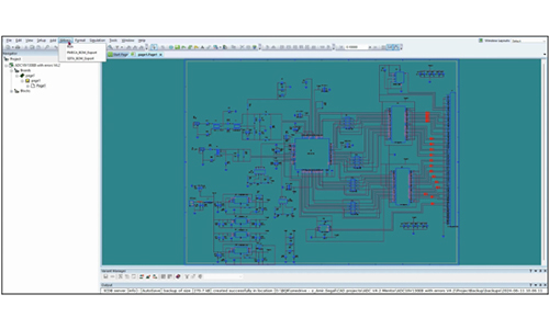
The Synthelyzer™ plugin integrates seamlessly with major ECAD tools such as Altium, OrCAD, and Mentor. This integration greatly reduces manual data entry and ensures that your analysis is traceable to the latest schematic design, streamlining your workflow.
Dynamic Linking and Synchronization
Synthelyzer™ delivers insightful feedback on design changes by leveraging the most current schematic data. The plugin ensures dynamic linking and synchronization with the latest schematic design in your ECAD tool, aligning design changes with analysis results. This capability allows you to swiftly identify and address potential electrical stress issues, enhancing the robustness of your design process and eliminating the risk of Electrostatic Over-Stress (EOS).
Detailed Reporting
The plugin generates comprehensive reports on stress derating and reliability metrics. These detailed reports assist with compliance to industry standards and regulatory requirements and provide valuable documentation for design reviews and certification processes.
Best Practices for Effective Electrical Stress Analysis
To maximize the effectiveness of electrical stress analysis, consider the following best practices.
Early Integration
Incorporate electrical stress analysis early in the PCB design process. Identifying potential issues at the outset allows for proactive resolution and minimizes the impact on development timelines.
Comprehensive Analysis
Conduct a thorough analysis that encompasses both electrical and thermal aspects of the PCB. Addressing all relevant factors ensures a more complete understanding of potential stress points and their implications.
Utilize Simulation Tools
Leverage simulation software to accurately predict component behavior and identify potential hotspots. Advanced tools provide detailed insights that are critical for optimizing design and preventing failures.
Consider Worst-Case Scenarios
Evaluate the impact of worst-case scenarios, such as maximum operating temperatures or sudden voltage surges. Assessing these conditions helps ensure that the design can withstand extreme situations and maintain reliable performance.
and FMECA Analysis Within Your ECAD During Board Design
Regular Updates
Keep your electrical stress analysis updated as design changes occur. Continuous alignment with the evolving design ensures that the analysis remains accurate and relevant throughout the development process.
Conclusion
Electrical stress analysis is an indispensable aspect of board design, ensuring the long-term reliability and safety of electronic devices. By understanding its principles, employing an effective tool like the Synthelyzer™ ECAD Plugin, and adhering to best practices, engineers can mitigate electrical overstress, enhance board performance, and achieve superior product reliability.
For further insights into how Synthelyzer™ can revolutionize your design process and elevate your stress analysis capabilities, visit Synthelyzer™ ECAD Plugin webpage.
Related Categories